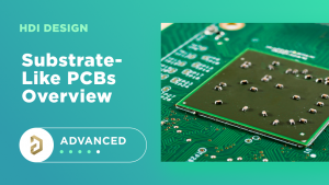
Higher Circuit Density in HDI PCBs
When you are designing a high-density circuit board (HDI PCB), there are many factors that must be taken into consideration. From determining the number of layers to choosing a stack-up, all of these details can affect your final product’s performance and functionality. The key to achieving higher circuit density in HDI PCBs is to select a design that utilizes smaller trace widths and via sizes. This can be accomplished through a variety of techniques, including via-in-pad (Via-in-Pad), blind and buried vias and other advanced via structures.
Whether you’re using V-in-Pad or a different process, it’s important to select the right material for your core and surface finish. The type of material you use will decide the thickness of your trace width, hole size and backup dimension. You’ll also need to take into account other elements, such as the location of the component pads, which will determine how much space you have for routing.
Another factor to consider is the amount of copper used on the traces. The more copper you use, the thicker your traces will be. This can impact the amount of space available for signaling, and can lead to crosstalk. The best way to minimize crosstalk is to route impedance-controlled traces. This can be achieved by ensuring that your trace width is consistent with the manufacturer’s DFM guidelines.
How to Achieve Higher Circuit Density in HDI PCBs
Achieving higher circuit density in hdi pcb requires the use of specialized materials and manufacturing techniques. These techniques include laser drilling for microvias and precise lamination processes. Because of this, traditional PCB fabrication methods are not suitable for the production of HDI boards.
There are several benefits to using HDI PCBs, including increased reliability and lower cost. This technology is ideal for applications that require a high level of connectivity, such as mobile devices and automotive electronics. Its compact design also allows it to fit into smaller spaces. It is also lightweight, which makes it easier to transport and store. In addition to increasing the number of components on a board, HDI PCBs can reduce the overall footprint and weight of the device. The smaller design can also help manufacturers save on materials and labor costs.
The main advantage of HDI PCBs is that they are more flexible than conventional PCBs. The smaller size makes them easy to transport and store, and they can be made from a wide range of materials. This flexibility makes them more versatile than standard PCBs and allows them to be used in a wider range of applications. In order to achieve a high level of circuit density in an HDI PCB, you must make sure that all of the components are placed properly on the board. This will depend on the type of components you choose, as well as the number of layers and the layout of the stack-ups.
The most common type of HDI PCBs is the 2+N+2 design. This type of HDI PCB has two layers of outer build up layers that are connected by a single layer of a core material. The outer layers of the build up layers can be plated with any of the following surface finishes: ENIG, HASL, immersion tin or gold. The core material can be FR4, metal or fiberglass.